There are Three Alternative For Packing of. By Mohamed Shoib October 4 2020 VLSI.

Vlsi Physical Design Home Facebook
DRT Tclk Tcapture clock logic Delay -Tsetup -Tuncrtaintyclock net delay for setup time analysis.
. Full Custom Standard Cell Gate Array and FPGAs. To check the fixed status of the cell. DbGet dbGet -p2 dbGet -p topinstspStatus fixedcellname invx1 11To report the core box.
This is the VLSI Very Large Scale Integration Design Course blog for VLSI Job aspirants. Xz VLSI I share my notes for learning Backend VLSI. VLSI physical design training in India Discover a new career that designed for you learn VLSI physical design course.
A blog to explore whole VLSI Design focused on ASIC Design flow Physical Design Signoff Standard cells Files system in VLSI industry EDA tools VLSI Interview guidance Linux and Scripting Insight of Semiconductor Industry and many more. The Art of Physical Design This blog will help you find all the essential articles needed for a beginner in the field of Physical DesignThis blog will be a collection of my ideasthoughts and resources based on my experience in technologyTopics that will be covered here includes VLSI Physical Design flow Static Timing AnalysisSTA Low Power concepts etcI wish to include. The design flow deals with various steps involved.
Here you can learn all the VLSI Physical Design concepts. Logical libraries lib db contain the info like delay power multiple timing arcs noise etc. Routed metal paths must meet timing clock.
Some of the blogs for PD which I found interesting are. Everything you can get to know about VLSI in general and physical design in particular. In backend there is no term called as wire load model.
A library is a collection of cells that forms a consistent hierarchy. We need to ensure that the design is stable across all corners to be specific in Tech terms PVT Corners Process Voltage Temperature. It is the result of a synthesized netlist that has been placed and routed.
It is one of the steps of physical verification. To get the dont touch attributes. Delay of a cell depends on input transition and output load.
VLSI- Physical Design For Freshers Learn physical design concepts in easy way and understand interview related question only for freshers. Join sumedhait for physical design course. Routing is the process of creating physical connections based on logical connectivity.
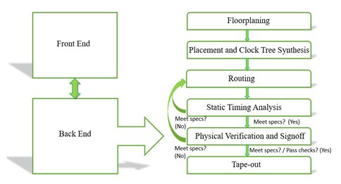
Skew max transcap requirements and also physical DRC requirements. Physical Design is a process of transforming a circuit description into physical layout which describes the position of cells and routes for the interconnections between them. Physical Design Flow.
2013-5-13 42wwwi-world-techblogspotin Physical design is one of the Steps in the VLSI design Cycle. When the synthesized design meets functionality timing power and other design goals you can pass the design to the IC Compiler or IC Compiler II tool. Timing analysis at back end requires knowledge of all clock related constraints provided at front end.
Welcome to Physical Design blog. Physical design is Further divided into Partitioning Floor Plan and Placement Routing Compaction Extraction and Verification. During the process flow of physical design prescribed Tool-Cadence synopsys etc MMMC file takes all relevant details.
Thursday February 26 2015. VLSI design can be modeled in either functional or test mode etc with each mode at varied process corners. While DRC only checks for certain layout rules to ensure the design will be manufactured reliably functional correctness of the design is ensured by LVS.
Blog - Physical design STA Synthesis DFT Automation Flow Dev Verification services. VLSI Physical Design crash course has been specially designed for those who aspire to be VLSI Semi custom ASIC Physical design engineer conducted by the real time industrial experienced professionals This fast track crash course will befit recently passed out engineering graduates as well as experienced professionals who would like to change career to. The main building blocks to design combinational and sequential circuits are logic gates which is explained below.
DAT Tlaunch TcqTcombonet delays. Electronics has also completely eliminated the Distance barrier throughout. Layout vs Schematic LVS compares the design.
A Design Compiler for logic synthesis which converts a design description written in a hardware description language such as Verilog or VHDL into an optimized gate-level netlist mapped to a specific logic library. Physical Design. The other one being DRC Design Rule Check.
When sdc file given to physical design tool like Astro its first object is to remove all Wire Load Models WLM which are used for front end timing analysis. Simple and easy to understand. This blog may help any electronic engineering graduate as well as experienced people and who is willing to join in Vlsi field.
A blog to explore whole VLSI Design focused on ASIC Design flow Physical Design Signoff Standard cells Files system in VLSI industry EDA tools VLSI Interview guidance Linux and Scripting Insight of Semiconductor Industry and many more. LVS stands for Layout vs Schematic. I work as a Physical Design Engineer.
There are basically two types of libraries namely physical and logical libraries. Pins are connected by routing metal interconnects. This blog provides insightful articles on VLSI and EDA domains ranging from frontend design to physical design.
Add to this is the COVID pandemic which has increased our dependence on gadgets to multifold. There are Four Major design Style. Understanding VLSI Integrated Circuit design.
There are four steps of routing operations. Sumedhait is the best VLSI physical design institute in India with a core objective to provide 100 job oriented course in VLSI Physical Design. For building hardware we need logic gates combinational circuits and sequential circuits which takes input in the form of binary numbers.
If you have any questions or thoughts please feel free to let me know. Data required time is the time taken by the signal from clock definition point to the clock pin of the capturing flop is called as the data required time. To report the power domain names.
VLSI Pro - Slick on Silicon 4. We hope you had a good understanding of Number Systems which is available Number Systems. In the world we live in Electronic Gadgets have become an inseparable part of our lives.
Delay of a cell will be calculated by lookup table approach if input. Posted by Prem kumar at 2262015 112100 PM 1 comment. VLSI PHYSICAL DESIGN FOR FRESHER will be helpful for the Physical design engineer and to find physical design engineer jobs.
Email ThisBlogThisShare to TwitterShare to FacebookShare to Pinterest.

Vlsi Physical Design
Vlsi Physical Design Methodology For Asic Development With A Flavor Of Ip Hardening

Team Vlsi Physical Design Flow In Details Asic Design Flow

Team Vlsi Inputs For Physical Design Physical Design Input Files

Asic System On Chip Vlsi Design Physical Design Flow

Top 15 Vlsi Blogs News Websites To Follow In 2022

Team Vlsi Pre Placement Activities In Physical Design

Vlsi Physical Design Flow Vlsi4freshers
0 comments
Post a Comment